Overview
Selective laser ablation is a widely utilized technique in industrial laser processing, prized for its ability to achieve high processing speeds while maintaining exceptional quality and precision. Using femtosecond laser pulses, small sections of metal layers can be precisely removed without damaging the substrate.
Physical Principle
Cold ablation occurs when pulse duration is shorter than electron-phonon coupling time. Material sublimates directly from solid to gas phase before thermal diffusion can occur. This enables selective removal of coatings, thin films, or surface layers with nanometer-level control.
Recommended CP-Series Models for This Process
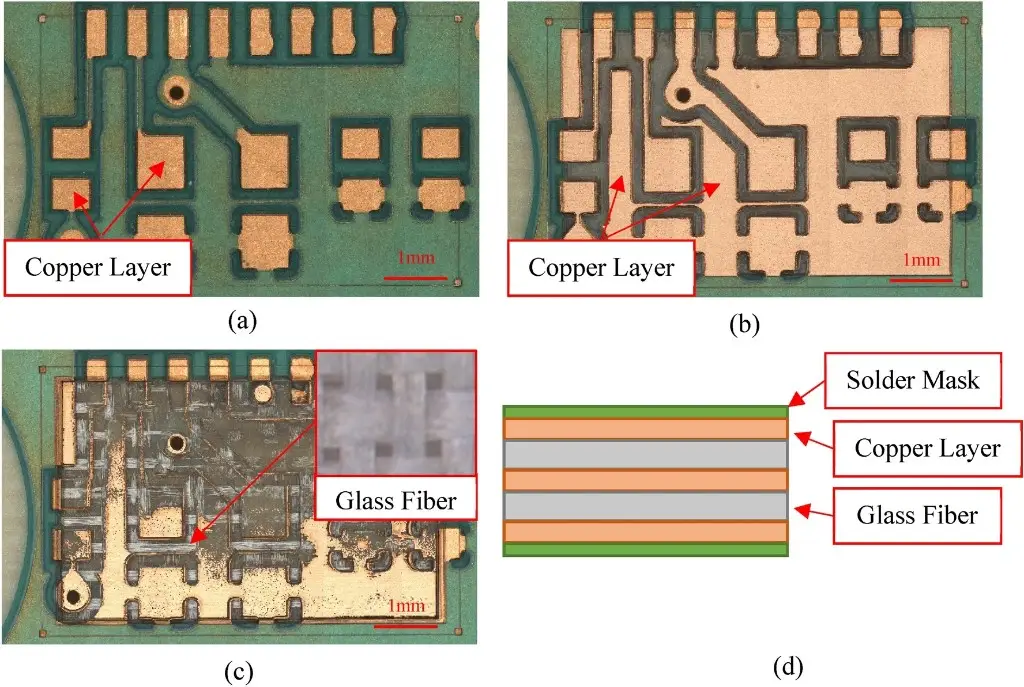
Femtosecond laser delayering of printed circuit board (PCB) for 3D volumetric imaging. (a) PCB surface showing copper layer before ablation, (b) partial ablation revealing underlying layers, (c) complete layer removal exposing glass fiber reinforcement, (d) cross-sectional schematic showing solder mask, copper layer, and glass fiber substrate structure. The femtosecond laser achieved selective material removal with minimal heat-affected zone, enabling high-resolution 3D reconstruction of multi-material PCB structures. Reproduced from Phoulady et al., Sci. Rep. 12, 12277 (2022). © 2022 The Authors. Licensed under CC BY 4.0.
Technical Capabilities
Compatible Materials
Metal coatings on polymers
Wire stripping, flex circuit processing
ITO (Indium Tin Oxide)
Display manufacturing, touchscreen patterning
Tungsten carbide
Cutting tool reconditioning
Paint and coating removal
Aerospace part refurbishment
Lithium battery electrodes
Cathode/anode patterning
Applications
Electronics Manufacturing
- •PCB trace correction
- •Flex circuit patterning
- •Wire insulation removal
Display Technology
- •ITO patterning for OLED
- •Pixel repair
- •Edge seal removal
Battery Manufacturing
- •Electrode tab formation
- •Cathode pattern ablation
- •Insulation layer removal
Surface Cleaning
- •Oxide layer removal
- •Contamination cleaning
- •Pre-weld surface prep
Technology Comparison
| Parameter | Femtosecond Ablation | Chemical Etching | Mechanical Abrasion |
|---|---|---|---|
| Selectivity | > 1000:1 | 10-100:1 | Poor |
| Substrate Damage | None | Possible | High risk |
| Feature Resolution | < 1 μm | 5-50 μm | > 100 μm |
| Environmental Impact | Minimal | Chemical waste | Particle debris |
| Automation | Fully automated | Batch process | Manual/semi-auto |
Related Application Spotlight
Ready to Implement This Process?
Contact us to discuss rental options (from €5000/month), outright purchase, or to connect with our partner network for job shop processing and process development services (paid).