Overview
Femtosecond laser dicing employs ultra-short laser pulses to create highly localized energy absorption within the material, resulting in minimal heat-affected zones and preventing thermal stress. This universal technique works across semiconductors, glass, ceramics, metals, and polymers—enabling precision separation that conventional blade dicing cannot achieve.
Physical Principle
The method allows for cleaner, more accurate cuts with smooth edges across virtually any material class. Cold ablation ensures no mechanical stress, no tool wear, and no subsurface damage—making it ideal for fragile, hard-to-cut, or high-value materials where maintaining the integrity of delicate structures is critical.
Recommended CP-Series Models for This Process
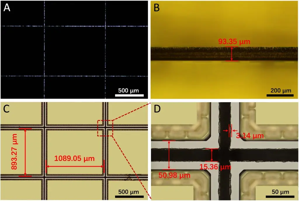
4-inch GaAs-based IC wafer cut into individual chips. (A) Die outlines visible on back side after full-thickness cutting, (B) measured die thickness 93.35 µm, (C) die dimensions 1089.05 × 893.27 µm, (D) kerf width 15.36 µm with minimized HAZ of 3.14 µm. Reproduced from Cai et al., Adv. Sci. 2025, 2515347. © 2025 The Authors. Published by Wiley-VCH GmbH under CC BY 4.0.
Technical Capabilities
Compatible Materials
Silicon (Si)
Stealth dicing, cleaner dies than blade
Silicon Carbide (SiC)
Enables dicing of hard semiconductor
Gallium Nitride (GaN)
Critical for power electronics
Sapphire substrates
LED and microLED production
Glass (borosilicate, fused silica)
Precision optics and microfluidics
Ceramics (LTCC, alumina)
Sensor and RF substrates
Diamond
Ultra-hard material separation
Polymers (PI, PEEK)
Flexible electronics and medical devices
Applications
Semiconductor Manufacturing
- •IC wafer singulation
- •Power device separation
- •MEMS die separation
Microelectronics
- •Thin wafer dicing (<50 μm)
- •Multi-layer stack dicing
- •Sensor die preparation
Photonics & Optics
- •Optical window dicing
- •Fiber array separation
- •Waveguide device singulation
Medical Devices
- •Ceramic implant separation
- •Polymer catheter cutting
- •Glass microfluidic chip dicing
Technology Comparison
| Parameter | Femtosecond Stealth Dicing | Blade Dicing | Plasma Dicing |
|---|---|---|---|
| Kerf Width | < 10 μm | 30-70 μm | 20-50 μm |
| Subsurface Damage | None | Present (SSD) | Minimal |
| Die Strength | Improved (+30%) | Standard | Good |
| Consumables | None | Blade wear | Plasma gas |
| Throughput | Medium-High | Very High | Medium |
Related Application Spotlight
Ready to Implement This Process?
Contact us to discuss rental options (from €5000/month), outright purchase, or to connect with our partner network for job shop processing and process development services (paid).