Laser Welding & Bonding
Hermetic Joining of Dissimilar Materials Without Adhesives
Overview
Femtosecond laser transmission welding enables direct bonding of transparent to opaque materials through highly localized heating at the interface. Unlike adhesive bonding, this creates a true fusion joint without intermediate layers, contamination risk, or aging degradation. The technology excels at joining dissimilar materials with drastically different thermal properties.
Physical Principle
The laser beam transmits through the transparent upper material and is absorbed at the interface or by the opaque lower substrate. Nonlinear multiphoton absorption can occur in the transparent material at the focal point, enabling bonding even between two transparent substrates without absorbing layers. Localized melting and resolidification create mechanical interlocking and chemical bonding.
Recommended CP-Series Models for This Process
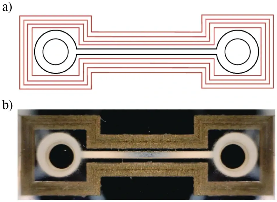
Femtosecond laser bonding of PMMA to silicon for hybrid microfluidic device. (a) CAD design of microfluidic channel connecting two reservoirs (red lines = PMMA structure, black circles = inlet/outlet ports), (b) optical microscopy of completed device showing successful sealing of channels with clean bonding seams visible as brown lines. The device was bonded with 2.0 μJ pulse energy at 800 kHz repetition rate and 1 mm/s scanning speed, achieving 0.44 MPa shear strength and passing pressure leak tests up to 1 bar. Reproduced from Conte Capodacqua et al., Sci. Rep. 13, 5062 (2023). © 2023 The Authors. Licensed under CC BY 4.0.
Technical Capabilities
Compatible Materials
PMMA to Silicon
Microfluidic devices, 0.44 MPa shear strength
Glass to Silicon
MEMS packaging, up to 85 MPa shear strength
Glass to Glass
Optical assemblies, hermetic sealing
Sapphire to Sapphire
High-temperature optical windows, hermetic sealing
Sapphire to Stainless Steel
Pressure sensors, high-temp viewports
Polymer to Polymer (PMMA-PMMA)
Lab-on-chip bonding
Silicon to Copper
Power electronics, 2.2 MPa shear strength
Applications
Microfluidic Devices
- •Lab-on-chip sealing
- •PMMA-silicon hybrid devices
- •Hermetic channel encapsulation
MEMS & Sensors
- •Wafer-level packaging
- •Pressure sensor sealing
- •Hermetic enclosures
Optical Assembly
- •Glass lens assembly
- •Prism bonding
- •Optical window sealing
Power Electronics
- •Semiconductor-metal joints
- •Heat sink attachment
- •Wire bonding alternatives
Technology Comparison
| Parameter | Femtosecond Laser Welding | Adhesive Bonding | Anodic Bonding |
|---|---|---|---|
| Bond Strength | 0.4-85 MPa | 5-30 MPa | 10-20 MPa |
| Precision | < 10 μm | 50-500 μm | Wafer-scale |
| Contamination Risk | None | High (outgassing) | Low |
| Aging/Degradation | Minimal | Significant | Minimal |
| Dissimilar Materials | Excellent | Good | Limited (requires ions) |
Related Application Spotlight
Application Spotlight: Femtosecond Glass-to-Metal Welding: What Makes the Joint Strong
An open-access Nanomaterials study on femtosecond pulse-burst welding of glass to mirror-polished metals maps how pulse energy, focal position, line spacing, and beam shape affect weld quality across glass-to-metal pairs for various industrial applications.
Read Application SpotlightApplication Spotlight: Burst-Mode Femtosecond Micromachining: Deeper, Straighter Holes in Glass
A Photoniques overview of MHz and GHz burst-mode ultrashort laser processing explains how pulse trains change ablation in metals and bandgap materials, enabling deeper cylindrical holes in glass and practical routes for milling, drilling, and cutting.
Read Application SpotlightReady to Implement This Process?
Contact us to discuss rental options (from €5000/month), outright purchase, or to connect with our partner network for job shop processing and process development services (paid).